by kamalnadh
STA:-
It is a method to determine if the circuit meets timing constraints without simulation.It provides faster and simple way of checking and analyzing all the timing paths in the design for any timing violations.
Advantages:-
Setup:-
It is the The minimum time required for the data to be stable before the clock edge.
 Fig:- Setup
Explanation:-
 Fig:- Hold
Explanation:-
STA:-
It is a method to determine if the circuit meets timing constraints without simulation.It provides faster and simple way of checking and analyzing all the timing paths in the design for any timing violations.
Advantages:-
- Speed.
- Exhaustive timing coverage.
- Capacity to handle full chip.
- Vector simulation is not required.
- It can report false errors.
- It is pessimistic.
- It is not suitable for asynchronous circuits.
- It can't detect errors related to logical operation.
- Netlist
- .lib
- Spef file
- .SDC(consrtaints)
Setup:-
It is the The minimum time required for the data to be stable before the clock edge.

Here we are considering two flip flops with same clock pulse.In above fig ff 1 sows the clock pulse of flip flop 1 and ff 2 shows the clock pulse of flip flop 2.For setup we should consider data path.The data is launched at ff 1 and captured at ff 2. The data is launched at rising edge of ff 1 and it should be captured before the next rising edge of the ff 2 clock.If the data is captured before the next rising edge then the time is beneficial.If the data is captured after the next rising edge then violations will occur these are called setup violations.
In simple words the data should capture with in full cycle.
Setup slack = Required time – Arrival time
Hold:-
The minimum time required for the data to be stable after the clock edge.

Here we are considering two flip flops with same clock pulse.In above fig ff 1 sows the clock pulse of flip flop 1.and ff 2 shows the clock pulse of flip flop 2.For hold we are considering clock path.Here the data is launched and captured at the same edge.If the data is captured after the clock edge of the ff 2 then the time is benefited.If the data is captured before the clock edge of the ff 2 then violations will occur.These are called hold violations.
In simple words the data should launch and capture at the same edge of the clocks.
 2. Multi cycle path:- It specifies the no of clock cycles required to propagate data from start to end of the path.


Hold slack = Arrival time – Required time
Data paths in STA:-
1.Input port to register
2.Register to register
3.Register to output
4.Input port to output port


Timing constraints:-
1.False path:- It specifies the logic path.In below fig when enable is 0 the output is 8( from first block 5 is active and from second block 3 is active 5+3=8) if we did't specifies the logic path tool will take wrong path like (5+5 or 3+3).
1.False path:- It specifies the logic path.In below fig when enable is 0 the output is 8( from first block 5 is active and from second block 3 is active 5+3=8) if we did't specifies the logic path tool will take wrong path like (5+5 or 3+3).


In above fig 2 cycles are used to propagate the data.
3.Min/Max delay:- It over ride the default setup and hold constraints with specific max and min time values
Latency (or) clock network delay (or) insertion delay:-
It is the time taken by the clock to reach the clock pin from the clock source.It is divided in to two types.Clock source latency and clock network latency.


Here from clock source to definition pin is the clock source latency.From the clock definition pin to clock pin of the flip flop 2 is the clock network latency.
Cell delay (or) propagation delay:-
cell delay is the amount of delay from input to output of of a logic gate in a path.
Net delay:-
It is the amount of the delay fro the output of cell to the input of next cell in the timing path.It is caused by the parasitic capacitance of the interconnection between two cells,combined with the net resistance and the limited drive strength of driving cell.
Drive strength:-
It is the capacity of the cell to drive a value to the cell connected to it's output.Small stranded cell have small capacitance and vice versa.It is easier to drive a small cell than large.
Transition delay (or) slope (or) wave delay (or) slew:-
Time taken to a signal to reach from 10% of vdd to 90% of vdd is called transition delay.

Clock uncertainty:-
It is the deviation of the actual arrival time of the clock edge with respect to ideal arrival time.The deviation happens mainly due to the jitter and noise.

In the fig above clock is normal.below clock is deviation of arrival time from it's ideal position.

Clock gating:-
It is the popular Technic used in many synchronous circuits foe reducing dynamic power dissipation.It saves power by adding more logic to a circuit to prune the clock tree.
OCV (on chip variation):-
The delay values of IC will varies in different conditions like changing in processor,voltage,temperature(PVT).The delay value of IC in cold weather is different and in hot weather is different.In cold weather the metals in ic will shrink.In hot weather the metal will expand so the delay will increase.To over come this effect flat derate(delay) is applied in the circuit.
In simple words OCV is a technique in this flat derate is applied to make faster path more fast and slower path more slow.Delays varies across a single die due to PVT(processor,voltage,temperature) .This need to be modeled by scaling the coefficients.
CRPR (clock re convergence pessimism removal):-
In this concept we removes the pessimism and derate to the common path.Generally we add the delay to every buffer in the process of OCV.But adding more delay is also effect the speed of the chip and it may cause violations to over come this we are removing the delay to the common path in the process of CRPR.
In simple words It can be used to remove the pessimism and penalty by using common cell for both launch and capture flip flop.
Derating:-
Timing derating factors models the effects of varying operating conditions by adjusting the delay values calculated for the individual timing arc of a block.
PVT operating conditions:-
PVT is to model inter chip variations. OCV is to model intra chip variations.
Process:- If the processor length is increases the delay also increases
Voltage:- If voltage is increases delay will reduces.
Temperature:-If temperature increases delay will increases.

Libraries in STA:-
1.Link lib:- It provides reference path
2.Target lib:-It is used for optimization
3.Symbolic lib:-It having symbols of cells(gates)
4.synthetic lib:- AOI and OAI combinations.
4.synthetic lib:- AOI and OAI combinations.
5.Design ware lib:-Provides the connectivity port.
6.physical lib:-It have shape of cells.
Skew:-
Difference between the two clock network delays is called skew.types of skews are given below.
Useful skew:-If the clock skew is intentionally added to meet the timing or reduce the violations this is called useful skew.
Local skew:-It is the difference in the arrival of clock signal at the clock pin of related flip flops.
Global skew:-It is the difference in the arrival of clock signal at the clock pin of non-related flip flops.
Global skew:-It is the difference in the arrival of clock signal at the clock pin of non-related flip flops.
Some definitions:-
Jitter:- Deviation of clock edge from it's ideal position.
Arrival time:-It is the time required for data travel through the data path.
Required time:-It is the time required for clock travel through the clock path.
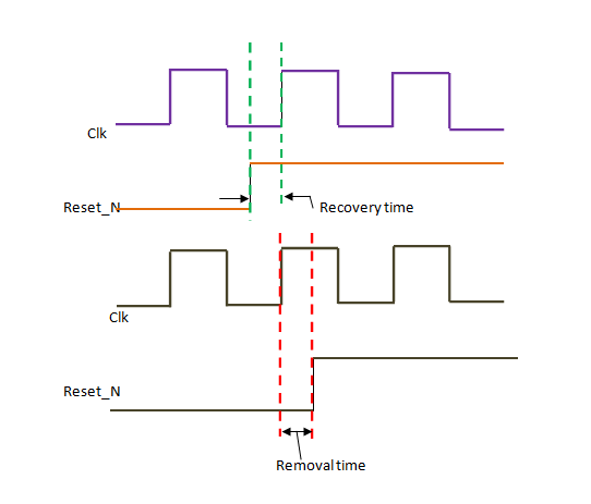
Recovery time:- It is the minimum time that an asynchronous control i/p pin must be stable after being deserted and before the next clock transition.
Removal time:- It is the minimum time that an asynchronous control input pin must be stable before being deserted and after the previous clock transition.
Arrival time:-It is the time required for data travel through the data path.
Required time:-It is the time required for clock travel through the clock path.
Recovery time:- It is the minimum time that an asynchronous control i/p pin must be stable after being deserted and before the next clock transition.
Removal time:- It is the minimum time that an asynchronous control input pin must be stable before being deserted and after the previous clock transition.

